
Digital Hardware Design CS 311
Lecture #4 , Jan 10th 2000

Contents
Incompletely Specified Functions
Why Incompletely Specified functions ?
Implementing Logic using MSI Blocks
Combinational MSI Blocks
Arithmetic MSI Units
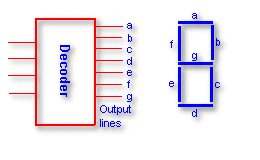
Decoders
Logic Implementation using Decoders
Multiplexer
Logic Implementation using Multiplexers
ROM ( Read Only memory )
Logic Implementation using ROM
PLA ( Programmable Logic Arrays )
Implementing logic using PLAs
Summary
Notes
In some cases , output need not be specified for all possible inputs.
Example : f(a,b,c,d) =![]() m(2,3,4,5,6,8,9) +
m(2,3,4,5,6,8,9) +![]() d(10,11,12,13,14,15)
d(10,11,12,13,14,15)
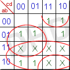
Here![]() m denotes the input
states for which the output is logic HIGH and
m denotes the input
states for which the output is logic HIGH and![]() d specifies the inputs for which the output can
be unspecified ( Don’t Care ). For rest output is zero.Now we
can minimise the K-Map as shown. Regarding the don’t care states
it is our choice whether the include them as 1 or 0. Usually they are
chosen so as to minimise the function.Some Don’t Cares may
remain 1 or 0.
d specifies the inputs for which the output can
be unspecified ( Don’t Care ). For rest output is zero.Now we
can minimise the K-Map as shown. Regarding the don’t care states
it is our choice whether the include them as 1 or 0. Usually they are
chosen so as to minimise the function.Some Don’t Cares may
remain 1 or 0.
Example:
In a BCD display certain inputs need not be specified like 10,11,12..15.
In this part of the lecture , implementation of Boolean functions
using MSI blocks will be covered. Medium Scale Integration (MSI)
devices have a complexity of approximately 10 to 200 gates in a single
package. They usually perform specific elementary digital functions
such as decoders , adders , and registers.
Various blocks available for implementing logic are :
Various blocks available for implementing arithmetic logic are :
Discrete quantities of information are represented in digital
computers with binary codes. A binary code of n bits is capable of
representing up to 2n distinct elements of the coded information. A
decoder is a combinational circuit that converts binary information
from the n coded inputs to a maximum of 2n unique outputs. If the
n-bits coded information has unused bit combinations , the decoder may
have less than 2n outputs.
The decoders presented in this section are called n-to-m line decoders
, where n <= 2n. Their purpose is to generate the 2n ( or fewer )
binary combinations of the n input variables. A decoder has n inputs
and 2n outputs and is also referred to as n to 2n decoder.
n to 2n Decoder
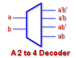
The logic diagram of a 2-to-4 decoder is shown. The two data
inputs are decoded into 4 outputs , each output representing one of
the combinations of the two binary input variables .Where required the
inputs are inverted and each of the AND gates generates one of the
binary combination ( See below ).
Partial
Decoding
Sometimes partial decoding may also be used i.e. not all the outputs
of the decoder may be needed. Eg. In a BCD display only a 4 to 10
decoder is needed .
Enable Input
Commercial decoders include one or more enable inputs to control the
operation of the circuit. The decoder is enabled when E is equal to 1
and disabled when E is equal to 0.
Implementation of
Circuit
The circuit for decoders is implemented in a fairly simple manner
:
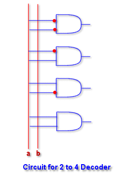
The outputs of the decoder are mutually exclusive i.e. only one of the
output can be logic 1 ( Assuming active high output ).
In some decoders active low output may also be there.
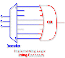
The above function is implemented using decoders in the above figure. Only the required outputs are fed to the OR gate as shown.
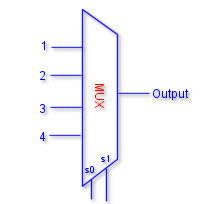
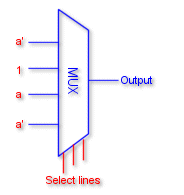
A multiplexer is a combinational circuit that receives binary
information from one of the 2n input data lines and directs it to a
single output line. The selection of a particular input data line for
the output is determined by a set of selection inputs. A 2n to 1
multiplexer has 2n input data lines and n input selection lines whose
bit combinations determine which input data are selected for the
output.
2n to 1 Multiplexers ( n select lines
)
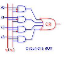
f(a,b,c) = ![]() m(0,1,3,5,6)
m(0,1,3,5,6)
Implementation of the above function is shown in the figure.
This implementation is not cost - efficient. See the next section for
a better implementation.
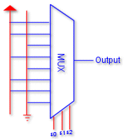
A new design :
In this design we use on of the inputs to feed the inputs of the
multiplexer instead of feeding it the select lines. This results in
usage of a much smaller multiplexer. Of course, some logic is usually
required when feeding the inputs of the multiplexer ( usually an
inverter for a single variable ).
As the name implies , a read-only memory ( ROM ) is a memory unit that performs the read operation only; it does not have a write capability. This implies that the binary information stored in a ROM is made permanent during the hardware production of the unit and cannot be altered by writing different words into it. Whereas a RAM is a general purpose device whose contents can be altered during the computational process , a ROM is restricted to reading words that are permanently stored within the unit. The binary information to be stored , specified by the designer , is then embedded in the unit to form the required interconnection pattern. ROMs come with special internal electronic fuses that can be "programmed" for a specific configuration. Once the pattern is established , it stays within the unit even when power is turned off and on again.

In ROM , the function is implemented directly. It is extremely
flexible and can be reprogrammed to represent an entirely different
function.
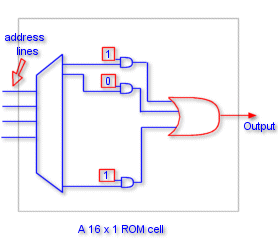
The above figure shows what is inside the ROM. Content of a ROM can be easily changed.
Multiple functions
More than one outputs can be got from the ROM by having n-bit cells
instead of 1 bit cells associated with each address line. Thus a n-bit
cell ROM will yield n outputs thus implementing n functions
simultaneously.
Introduction :
PLAs belong to a class of components called programmable
logic devices or PLDs , a term applied to ICs containing many gates or
other general - purpose cells whose interconnections can be configured
or "programmed" to implement any desired combinational or sequential
function. PLDs are relatively easy to design and inexpensive to
manufacture. They constitute a key technology for building
application-specific integrated circuits (ASICs).
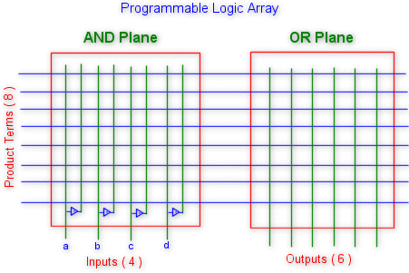
The programmable logic array ( PLA ) shown in the figure is intended
to realise a set of combinational logic functions in minimal SOP form.
It consists of an array of AND gates ( the AND plane ) , which realise
a set of product terms , and a set of OR gates ( the OR plane ) ,
which form various logical sums of the product terms. The inputs to
the AND gates are programmable and include all the input variables and
their complements. Hence it is possible to program any desired product
term into any row of the PLA.
PLA specification : n x k x m
( n inputs , k product terms and m outputs )
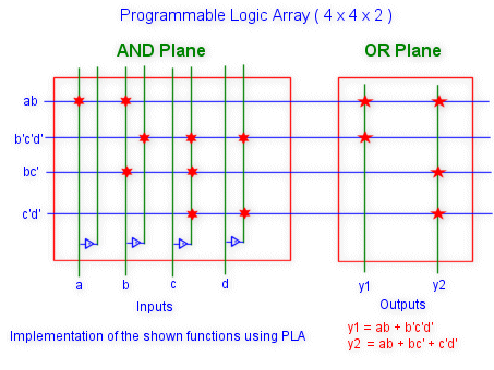
To implement a n-variable function ( with k minterms ) we have the
following options available with us :
 |
Notes Compiled and presented by Ashish Gupta ashishgupta@pinkfloyd.com
|
Notes :